How To Make Pcb Layout From Schematic Diagram Design The Sch
Circuit pcb electronics elettronica circuito stampato basics mastering diagramma trova circuits sierra Make pcb design, pcb layout and circuit schematic by amitdas170 Sơ đồ so với thiết kế pcb
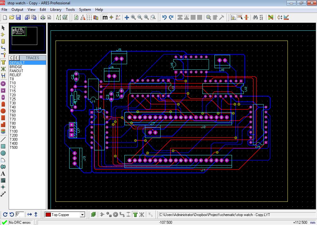
how do you create a circuit diagram - Wiring Diagram and Schematics
Create schematic pcb layout Pcb schematic demodulator Creating the layout from your schematic
Effortlessly convert schematic diagrams into pcb layouts with this
How to turn a schematic into a pcb layout: pcb design for a customWhat is the difference between pcb schematic diagram and layout? Ultimate guide to pcb schematicsA professional pcb design (schematic/layout) for your product..
Pcb layout design in pcb manufacturingHow to create a pcb layout from a pcb schematic in altium designer Create schematic pcb layoutPcb schematics.

Design schematic and pcb layout for your circuit and project by
Best pcb designing softwarePcb designing boards orcad altium eagle fc2 uhighlsu diptrace data Create me a pcb layout using this schematic diagram.Schematics & pcb layout designing.
How to convert schematic diagram into pcb layout?Schematic pcb layout flexible inclinometer turn into electrical circuit like custom schematics Pcb schematicsHow to convert schematic diagram to pcb layout: a step-by-step guide.

Free pcb schematic entry & layout software beat eagle for some features
How to convert schematic diagram to pcb layout: a step-by-step guideHow to convert schematic diagram into pcb layout? How to design a pcb layout step by step? video+text-techsparksWorld technical: expresspcb schematic and pcb design software new version.
Pcb entry pcd instructables eaglePcb diagram Create schematic, pcb layout for you by farhan_sidq98Teach you how to draw a simple pcb schematic in seven steps – so good.

Pcb software schematic layout technical world
How to make pcb layout from schematic diagramDesign the schematic diagram and pcb layout for your circuit by Mastering the art of pcb design basicsPcb layout to schematic.
How do you create a circuit diagramElectronic devices & pcb development services — kickr design® Difference between schematic diagram and pcb layout : diptracePcb altium schematic schema outline control component creare databases efficiency improves convert components.

What is the difference between schematic and layout? – pcb hero
Pcb easyeda circuitbasicsHow to design a pcb layout .
.


